- 您现在的位置:买卖IC网 > Sheet目录319 > COP8SG-EPU (National Semiconductor)BOARD PROTOTYPE/TARGET COP8
Reset
(Continued)
R1
R2
C1
C2
CKI Freq
Conditions
(k ? )
(M ? )
(pF)
(pF)
(MHz)
0
0
1
1
30
200
30–36
100–150
4
0.455
V CC = 5V
V CC = 2.5V
TABLE 2. RC Oscillator Configuration, T A = 25?C
R
(k ? )
C
(pF)
CKI Freq
(MHz)
Instr. Cycle
(μs)
Conditions
DS012829-7
3.3
82
2.2 to 2.7
3.7 to 4.6
V CC = 5V
RC
> 5 x Power Supply Rise Time
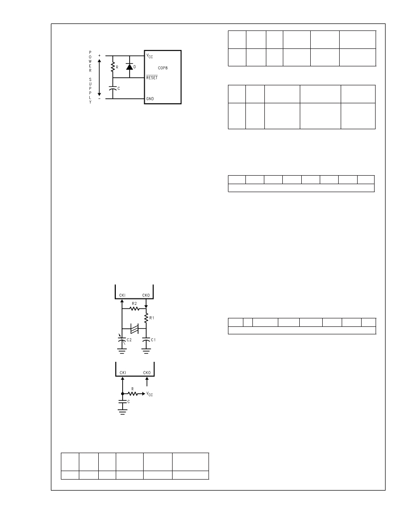
FIGURE 6. Recommended Reset Circuit
5.6
6.8
100
100
1.1 to 1.3
0.9 to 1.1
7.4 to 9.0
8.8 to 10.8
V CC = 5V
V CC = 5V
Oscillator Circuits
The chip can be driven by a clock input on the CKI input pin
which can be between DC and 10 MHz. The CKO output
clock is on pin G7 (crystal configuration). The CKI input fre-
quency is divided down by 10 to produce the instruction
cycle clock (1/t c ).
Note: 3k ≤ R ≤ 200k
50 pF ≤ C ≤ 200 pF
CONTROL REGISTERS
CNTRL Register (Address X'00EE)
Figure 7 shows the Crystal and R/C oscillator diagrams.
T1C3
T1C2
T1C1
T1C0
MSEL
IEDG
SL1
SL0
Bit 7
Bit 0
CRYSTAL OSCILLATOR
CKI and CKO can be connected to make a closed loop crys-
tal (or resonator) controlled oscillator.
Table 1 shows the component values required for various
standard crystal values.
R/C OSCILLATOR
By selecting CKI as a single pin oscillator input, a single pin
R/C oscillator circuit can be connected to it. CKO is available
as a general purpose input, and/or HALT restart input.
Table 2 shows the variation in the oscillator frequencies as
functions of the component (R and C) values.
The Timer1 (T1) and MICROWIRE/PLUS control register
contains the following bits:
T1C3 Timer T1 mode control bit
T1C2 Timer T1 mode control bit
T1C1 Timer T1 mode control bit
T1C0 Timer T1 Start/Stop control in timer
modes 1 and 2, T1 Underflow Interrupt
Pending Flag in timer mode 3
MSEL Selects G5 and G4 as MICROWIRE/PLUS
signals SK and SO respectively
IEDG External interrupt edge polarity select
(0 = Rising edge, 1 = Falling edge)
SL1 & SL0 Select the MICROWIRE/PLUS clock divide
by (00 = 2, 01 = 4, 1x = 8)
PSW Register (Address X'00EF)
HC
C
T1PNDA
T1ENA
EXPND
BUSY
EXEN
GIE
Bit 7
The PSW register contains the following select bits:
HC Half Carry Flag
Bit 0
DS012829-8
DS012829-9
FIGURE 7. Crystal and R/C Oscillator Diagrams
TABLE 1. Crystal Oscillator Configuration, T A = 25?C
C Carry Flag
T1PNDA Timer T1 Interrupt Pending Flag (Autoreload
RA in mode 1, T1 Underflow in Mode 2, T1A
capture edge in mode 3)
T1ENA Timer T1 Interrupt Enable for Timer Underflow
or T1A Input capture edge
EXPND External interrupt pending
BUSY MICROWIRE/PLUS busy shifting flag
EXEN Enable external interrupt
GIE Global interrupt enable (enables interrupts)
The Half-Carry flag is also affected by all the instructions that
affect the Carry flag. The SC (Set Carry) and R/C (Reset
Carry) instructions will respectively set or clear both the carry
R1
(k ? )
0
R2
(M ? )
1
C1
(pF)
30
C2
(pF)
30–36
CKI Freq
(MHz)
10
Conditions
V CC = 5V
flags. In addition to the SC and R/C instructions, ADC,
SUBC, RRC and RLC instructions affect the Carry and Half
Carry flags.
www.national.com
18
发布紧急采购,3分钟左右您将得到回复。
相关PDF资料
CORE1553-DEV-KIT
KIT DEVELOPMENT FOR IP CORE1553
CP131-AG
LNR PWR SUP 5V 8A, +/-12V 1.7A
CPC1590P
MOSFET GATE DVR ISO 8-FLATPACK
CPC5002G
ISOLAT DGTL 3.75KVRMS 2CH 8-DIP
CPCI-D-3U-300C
PWR SUPLY DC/DC CPCI 300W 3UX8HP
CPD250-4530G
PWR SUP 250W 3.3/5/12/-12V QUAD
CS4161YN8
IC DRIVER H-BRDG DUAL 85MA 8DIP
CS5461A-ISZ
IC ENERGY METERING 1PHASE 24SSOP
相关代理商/技术参数
COP8SGR728M7
功能描述:8位微控制器 -MCU RoHS:否 制造商:Silicon Labs 核心:8051 处理器系列:C8051F39x 数据总线宽度:8 bit 最大时钟频率:50 MHz 程序存储器大小:16 KB 数据 RAM 大小:1 KB 片上 ADC:Yes 工作电源电压:1.8 V to 3.6 V 工作温度范围:- 40 C to + 105 C 封装 / 箱体:QFN-20 安装风格:SMD/SMT
COP8SGR728M7/NOPB
功能描述:8位微控制器 -MCU RoHS:否 制造商:Silicon Labs 核心:8051 处理器系列:C8051F39x 数据总线宽度:8 bit 最大时钟频率:50 MHz 程序存储器大小:16 KB 数据 RAM 大小:1 KB 片上 ADC:Yes 工作电源电压:1.8 V to 3.6 V 工作温度范围:- 40 C to + 105 C 封装 / 箱体:QFN-20 安装风格:SMD/SMT
COP8SGR728M8
功能描述:8位微控制器 -MCU RoHS:否 制造商:Silicon Labs 核心:8051 处理器系列:C8051F39x 数据总线宽度:8 bit 最大时钟频率:50 MHz 程序存储器大小:16 KB 数据 RAM 大小:1 KB 片上 ADC:Yes 工作电源电压:1.8 V to 3.6 V 工作温度范围:- 40 C to + 105 C 封装 / 箱体:QFN-20 安装风格:SMD/SMT
COP8SGR728M8/NOPB
功能描述:8位微控制器 -MCU RoHS:否 制造商:Silicon Labs 核心:8051 处理器系列:C8051F39x 数据总线宽度:8 bit 最大时钟频率:50 MHz 程序存储器大小:16 KB 数据 RAM 大小:1 KB 片上 ADC:Yes 工作电源电压:1.8 V to 3.6 V 工作温度范围:- 40 C to + 105 C 封装 / 箱体:QFN-20 安装风格:SMD/SMT
COP8SGR728N8
功能描述:8位微控制器 -MCU RoHS:否 制造商:Silicon Labs 核心:8051 处理器系列:C8051F39x 数据总线宽度:8 bit 最大时钟频率:50 MHz 程序存储器大小:16 KB 数据 RAM 大小:1 KB 片上 ADC:Yes 工作电源电压:1.8 V to 3.6 V 工作温度范围:- 40 C to + 105 C 封装 / 箱体:QFN-20 安装风格:SMD/SMT
COP8SGR728N8/NOPB
功能描述:8位微控制器 -MCU RoHS:否 制造商:Silicon Labs 核心:8051 处理器系列:C8051F39x 数据总线宽度:8 bit 最大时钟频率:50 MHz 程序存储器大小:16 KB 数据 RAM 大小:1 KB 片上 ADC:Yes 工作电源电压:1.8 V to 3.6 V 工作温度范围:- 40 C to + 105 C 封装 / 箱体:QFN-20 安装风格:SMD/SMT
COP8SGR740N8
功能描述:IC MCU 8BIT CMOS OTP 40DIP RoHS:否 类别:集成电路 (IC) >> 嵌入式 - 微控制器, 系列:COP8™ 8SG 其它有关文件:STM32F101T8 View All Specifications 特色产品:STM32 32-bit Cortex MCUs 标准包装:490 系列:STM32 F1 核心处理器:ARM? Cortex?-M3 芯体尺寸:32-位 速度:36MHz 连通性:I²C,IrDA,LIN,SPI,UART/USART 外围设备:DMA,PDR,POR,PVD,PWM,温度传感器,WDT 输入/输出数:26 程序存储器容量:64KB(64K x 8) 程序存储器类型:闪存 EEPROM 大小:- RAM 容量:10K x 8 电压 - 电源 (Vcc/Vdd):2 V ~ 3.6 V 数据转换器:A/D 10x12b 振荡器型:内部 工作温度:-40°C ~ 85°C 封装/外壳:36-VFQFN,36-VFQFPN 包装:托盘 配用:497-10030-ND - STARTER KIT FOR STM32497-8853-ND - BOARD DEMO STM32 UNIV USB-UUSCIKSDKSTM32-PL-ND - KIT IAR KICKSTART STM32 CORTEXM3497-8512-ND - KIT STARTER FOR STM32F10XE MCU497-8505-ND - KIT STARTER FOR STM32F10XE MCU497-8304-ND - KIT STM32 MOTOR DRIVER BLDC497-6438-ND - BOARD EVALUTION FOR STM32 512K497-6289-ND - KIT PERFORMANCE STICK FOR STM32MCBSTM32UME-ND - BOARD EVAL MCBSTM32 + ULINK-MEMCBSTM32U-ND - BOARD EVAL MCBSTM32 + ULINK2更多... 其它名称:497-9032STM32F101T8U6-ND
COP8SGR740N8/NOPB
制造商:Texas Instruments 功能描述: